- 您现在的位置:买卖IC网 > Sheet目录1992 > CY284108ZXC (Silicon Laboratories Inc)IC CLOCK SERV CK410B 56TSSOP
CY284108
........................ Document #: 38-07713 Rev. *B Page 7 of 16
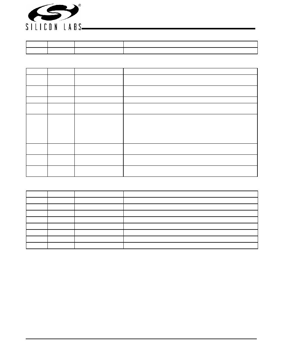
0
RESERVED
Byte 6: Control Register 6
Bit
@Pup
Name
Description
7
0
TEST_SEL
REF/N or Tri-state Select
0 = Tri-state, 1 = REF/N Clock
6
0
TEST_MODE
Test Clock Mode Entry Control
0 = Normal operation, 1 = REF/N or Tri-state mode
5
0
RESERVED
RESERVED, Set = 0
4
1
REF
REF Output Drive Strength
0 = Low, 1 = High
3
1
PCI_Stop Control
SW PCI_STP# Function
0 = SW PCI_STP# assert, 1 = SW PCI_STP# deassert
When this bit is set to 0, all STOPPABLE PCI, PCIF and SRC outputs will
be stopped in a synchronous manner with no short pulses.
When this bit is set to 1, all STOPPED PCI, PCIF and SRC outputs will
resume in a synchronous manner with no short pulses.
2
HW
FS_C
FS_C Reflects the value of the FS_C pin sampled on power up
0 = FS_C was low during VTT_PWRGD# assertion
1
HW
FS_B
FS_B Reflects the value of the FS_B pin sampled on power up
0 = FS_B was low during VTT_PWRGD# assertion
0
HW
FS_A
FS_A Reflects the value of the FS_A pin sampled on power up
0 = FS_A was low during VTT_PWRGD# assertion
Byte 7: Vendor ID
Bit
@Pup
Name
Description
7
0
Revision Code Bit 3
6
0
Revision Code Bit 2
5
0
Revision Code Bit 1
4
0
Revision Code Bit 0
3
1
Vendor ID Bit 3
2
0
Vendor ID Bit 2
1
0
Vendor ID Bit 1
0
Vendor ID Bit 0
Byte 5: Control Register 5 (continued)
Bit
@Pup
Name
Description
发布紧急采购,3分钟左右您将得到回复。
相关PDF资料
CY28410OXC-2
IC CLOCK CK410 GRANTSDALE 56SSOP
CY28410OXC
IC CLOCK CK410 GRANTSDALE 56SSOP
CY28411ZXC
IC CLOCK CK410M ALVISO 56TSSOP
CY28442ZXC-2
IC CLOCK ALVISO PENTM 56TSSOP
CY28445LFXC-5
IC CLOCK CALISTOGA CK410M 68QFN
CY28446LFXC
IC CLOCK CALISTOGA CK410M 64QFN
CY28447LFXC
IC CLOCK CALISTOGA CK410M 72QFN
CY28547LFXCT
IC CLOCK CK505/410M INTEL 72QFN
相关代理商/技术参数
CY284108ZXCT
功能描述:时钟发生器及支持产品 Server, CK410B RoHS:否 制造商:Silicon Labs 类型:Clock Generators 最大输入频率:14.318 MHz 最大输出频率:166 MHz 输出端数量:16 占空比 - 最大:55 % 工作电源电压:3.3 V 工作电源电流:1 mA 最大工作温度:+ 85 C 安装风格:SMD/SMT 封装 / 箱体:QFN-56
CY28410OC
制造商:SPECTRALINEAR 制造商全称:SPECTRALINEAR 功能描述:Clock Generator for Intel Grantsdale Chipset
CY28410OCT
制造商:SPECTRALINEAR 制造商全称:SPECTRALINEAR 功能描述:Clock Generator for Intel Grantsdale Chipset
CY28410OXC
功能描述:时钟发生器及支持产品 SysClk Intel Lakeprt & Grantsdale Chipset RoHS:否 制造商:Silicon Labs 类型:Clock Generators 最大输入频率:14.318 MHz 最大输出频率:166 MHz 输出端数量:16 占空比 - 最大:55 % 工作电源电压:3.3 V 工作电源电流:1 mA 最大工作温度:+ 85 C 安装风格:SMD/SMT 封装 / 箱体:QFN-56
CY28410OXC-2
功能描述:时钟发生器及支持产品 SysClk Intel Lakeprt & Grantsdale Chipset RoHS:否 制造商:Silicon Labs 类型:Clock Generators 最大输入频率:14.318 MHz 最大输出频率:166 MHz 输出端数量:16 占空比 - 最大:55 % 工作电源电压:3.3 V 工作电源电流:1 mA 最大工作温度:+ 85 C 安装风格:SMD/SMT 封装 / 箱体:QFN-56
CY28410OXC-2T
功能描述:时钟发生器及支持产品 SysClk Intel Lakeprt & Grantsdale Chipset RoHS:否 制造商:Silicon Labs 类型:Clock Generators 最大输入频率:14.318 MHz 最大输出频率:166 MHz 输出端数量:16 占空比 - 最大:55 % 工作电源电压:3.3 V 工作电源电流:1 mA 最大工作温度:+ 85 C 安装风格:SMD/SMT 封装 / 箱体:QFN-56
CY28410OXCT
功能描述:时钟发生器及支持产品 SysClk Intel Lakeprt & Grantsdale Chipset RoHS:否 制造商:Silicon Labs 类型:Clock Generators 最大输入频率:14.318 MHz 最大输出频率:166 MHz 输出端数量:16 占空比 - 最大:55 % 工作电源电压:3.3 V 工作电源电流:1 mA 最大工作温度:+ 85 C 安装风格:SMD/SMT 封装 / 箱体:QFN-56
CY28410ZC
制造商:SPECTRALINEAR 制造商全称:SPECTRALINEAR 功能描述:Clock Generator for Intel Grantsdale Chipset